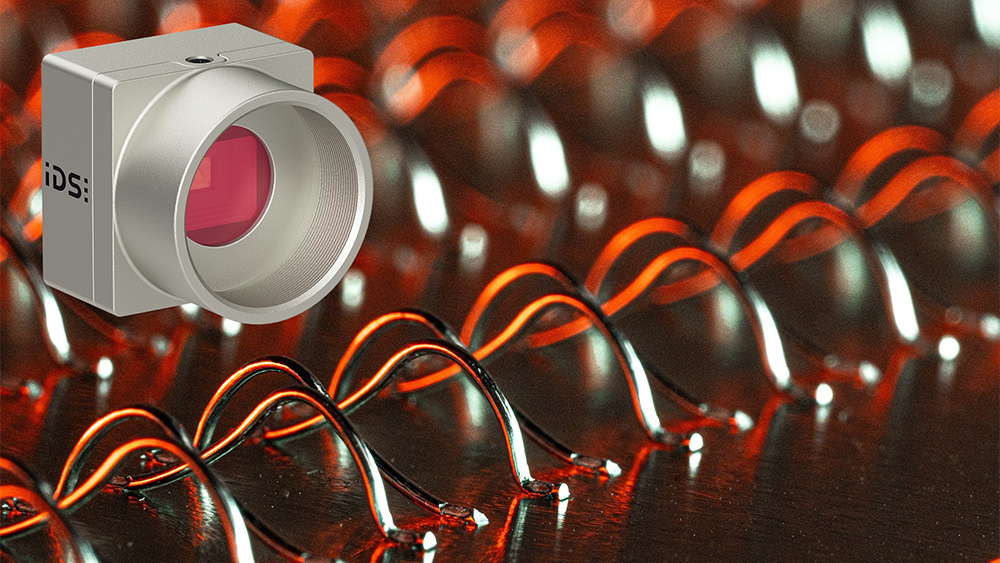
Wire bonding is a key process in semiconductor production. Extremely fine wires with diameters of 15 to 75 µm are used to create tiny electrical connections between a semiconductor chip and other components. The distances between the bond wires are often less than 100 µm. Any deviation, however small, can lead to connection errors. Therefore, wire bonding requires the highest precision and forms the basis for the production of high-performance electronics that are used in many different applications.
|
ADVERTISEMENT |
F&S Bondtec Semiconductor from Braunau, Austria, relies on image-processing technology with industrial cameras from IDS Imaging Development Systems for precisely determining wire positions and for quality assurance.
F&S Bondtec covers the desktop bonder and tester segment worldwide, offering a wide range of production and test equipment. It extends to the desktop microfactory, which combines all wire-bonding processes and test methods in one machine base. Since the company was founded in 1994, several thousand wire bonders and bond testers have left the factory and are in use in many laboratories, development departments, pilot production lines, and production facilities around the world.
…
Add new comment